
From schematic to tested PCB, step by step
Each stage follows an agreed technical scope and approved file revisions. We clarify the required inputs and handover before moving to the next step.
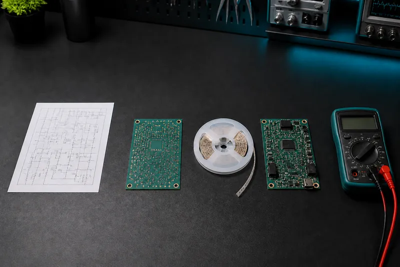
1. Schematic
We collect functional, power and installation requirements. The schematic and BOM provide a reviewable basis for the circuit.
2. PCB layout
Components are placed and connections routed. We review the board outline, connectors and production data for approval.
3. Partner manufacturing
Boards are manufactured by production partners from approved files, then checked. Technical queries are resolved before ordering.
4. Assembly
The BOM and placement file guide sourcing and SMT assembly. Orientations and the assembled board are checked.
5. Bring-up and testing
We check the power rails, load the agreed firmware and test the defined functions. Results and open issues are documented at handover.
Continue your project
Frequently asked questions
What should I send if I have a design?
Send the schematic, Gerber files, BOM and placement data from the same revision, plus quantity and the functions to test.
Can you join a project partway through?
Yes. We review the available documents and agree missing inputs and the scope of responsibility first.
Tell us about your electronics project
Send the available files, required functions and quantity. We will clarify the scope before preparing a proposal.