
PCB design from schematic to layout
We start with what the circuit needs to do. Power, signals, connectors and available space shape the schematic and board layout, with review points agreed before design begins.
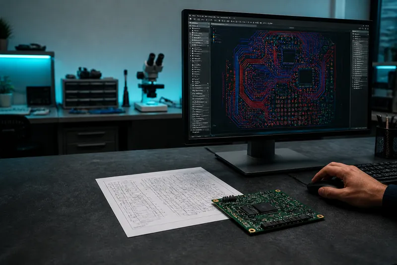
Schematics built around your requirements
We review interfaces, power needs and component availability. The schematic separates power, control and interfaces, with test points and programming access considered early.
Placement and routing
Board outlines, mounting points and connector locations guide placement. Routing follows the electrical loads, signal requirements and agreed manufacturing rules.
Files for the next stage
The reviewed design is handed over with versioned Gerber and drill files, a bill of materials and assembly data where required. We can then arrange a prototype or partner manufacturing.
Continue your project
Frequently asked questions
Can you work from an existing schematic?
Yes. Send the source files and bill of materials, along with board dimensions, connector constraints and intended use.
Can I request design only?
Yes. We agree the source documents and production files included in the proposal; manufacturing can be arranged separately.
Tell us about your electronics project
Send the available files, required functions and quantity. We will clarify the scope before preparing a proposal.
PCB layer stack
Illustrative layer structure.
- Top silkscreen
- Top solder mask
- Top copper
- FR4 substrate
- Bottom copper
- Bottom solder mask