
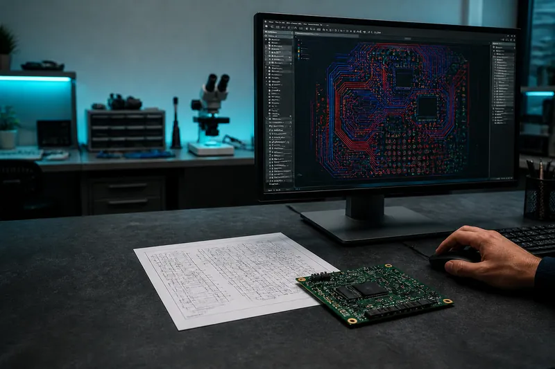
Schematic to PCB
We start with what the circuit needs to do. Power, signals, connectors and available space shape the schematic and board layout, with review points agreed before design begins.
Explore the service ↗Schematic → PCB layout → manufacturing through production partners → component sourcing and SMT assembly → bring-up and testing. One coordinated path for your electronics project.
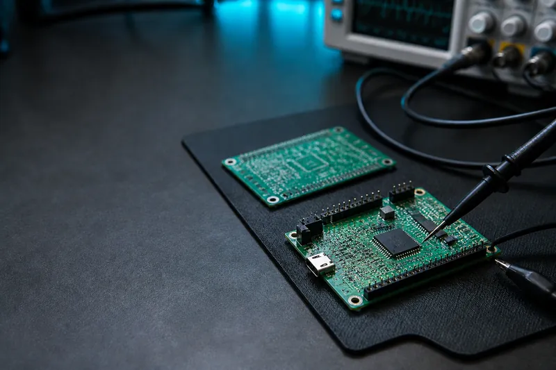
We start with what the circuit needs to do. Power, signals, connectors and available space shape the schematic and board layout, with review points agreed before design begins.
Explore the service ↗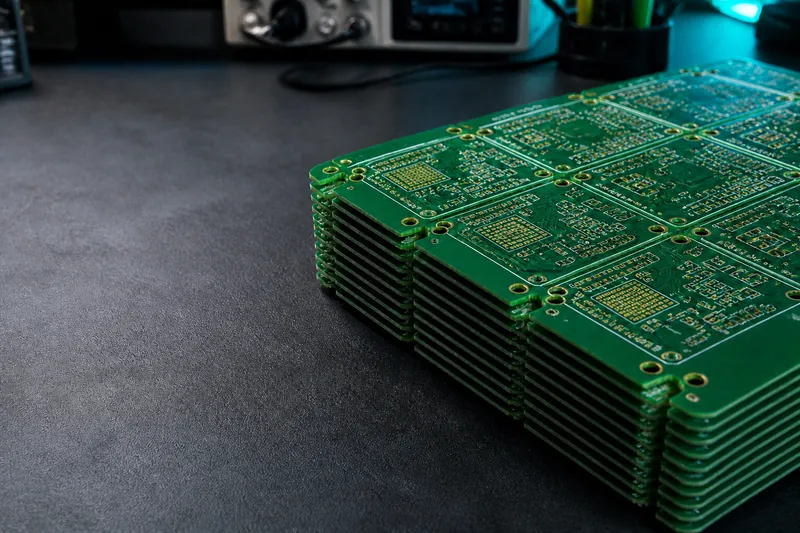
We arrange manufacturing through partner suppliers and check the boards. You have one contact for technical preparation, production queries and the handover to assembly.
Explore the service ↗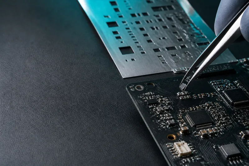
Assembly turns a bare board into a circuit. We align the bill of materials, placement data and first power-up procedure before work begins.
Explore the service ↗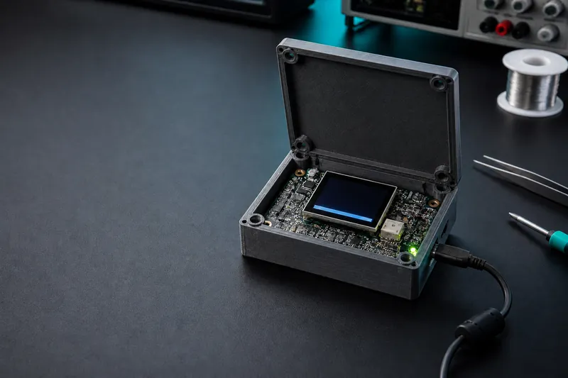
We turn the device’s purpose into testable requirements. Hardware, firmware and the installation environment are considered together from the outset.
Explore the service ↗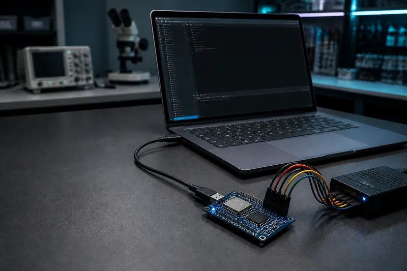
Firmware connects the board’s peripherals to the device’s purpose. Functions, communication and fault handling are designed alongside the hardware.
Explore the service ↗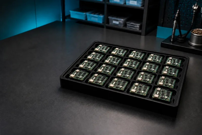
Once a prototype works, repeatability becomes the next task. We record board, BOM and firmware revisions and agree the acceptance criteria for the batch.
Explore the service ↗We collect functional, power and installation requirements. The schematic and BOM provide a reviewable basis for the circuit.
Components are placed and connections routed. We review the board outline, connectors and production data for approval.
Boards are manufactured by production partners from approved files, then checked. Technical queries are resolved before ordering.
The BOM and placement file guide sourcing and SMT assembly. Orientations and the assembled board are checked.
We check the power rails, load the agreed firmware and test the defined functions. Results and open issues are documented at handover.
Illustrative layer structure.
Illustration of the testing process.
Send the source and a readable PDF, with the board dimensions and connector constraints.
Include drill data, exact component numbers and placement data from the same revision.
Show connectors and labels, and describe what works and what needs changing.
List functions, power supply, interfaces, quantity and the checks you need.
Yes. Describe the intended use, power source, interfaces and main functions. We can define the schematic and layout together.
We arrange manufacturing with production partners and check the boards. We coordinate preparation, sourcing, assembly and agreed testing.
Yes. ESP32 and STM32 firmware development can be coordinated with the hardware and prototype tests.
Include your requirements, quantity and any schematic, Gerber, BOM or placement data you already have. A prototype photo is also helpful.
Tell us where your project stands and what you need next.